Based on contributions by Ihsan.
This is a quick-start guide to schematic capture and PCB layout in KiCad. It covers the basic project workflow; for anything beyond a simple board, refer to the official KiCad documentation.
What you need
- A computer running Windows, macOS, or Linux
- KiCad (installation is a standard, straightforward installer)
Steps
1. Create a new project
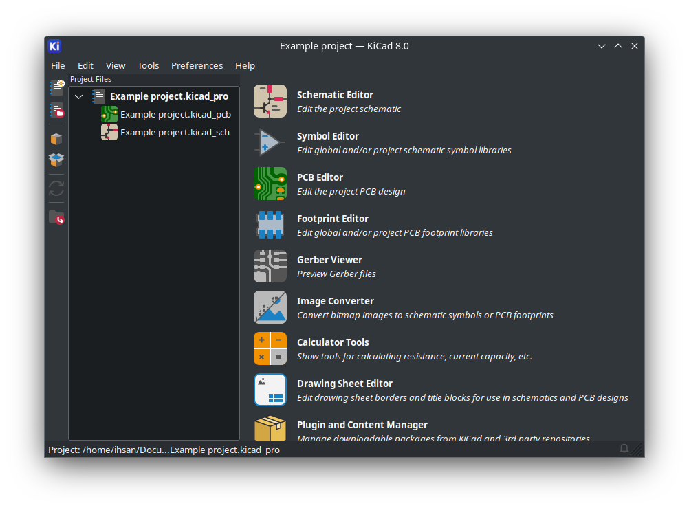
Open KiCad, go to File → New Project, and name your project.
2. Create the schematic
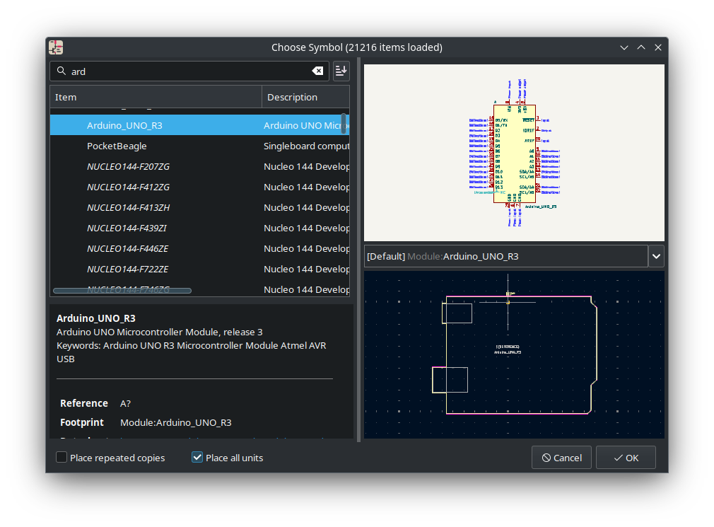
Open <your project name>.kicad_sch. Add components by clicking Add Symbol or pressing A. The symbol library is organized hierarchically, with symbols grouped by type, function, or manufacturer (e.g. Device, Resistor, Transistor, Microcontroller). See the schematic editor (eeschema) docs for details.
3. Assign footprints
Once you’ve picked the right symbol for a component, it usually won’t have a footprint assigned yet. A footprint is the physical “blueprint” of where the component sits and connects on the PCB.
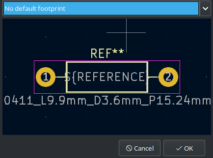
For generic components, pick a footprint from the dropdown. Make sure the footprint’s dimensions match your actual component.
4. Wire the schematic
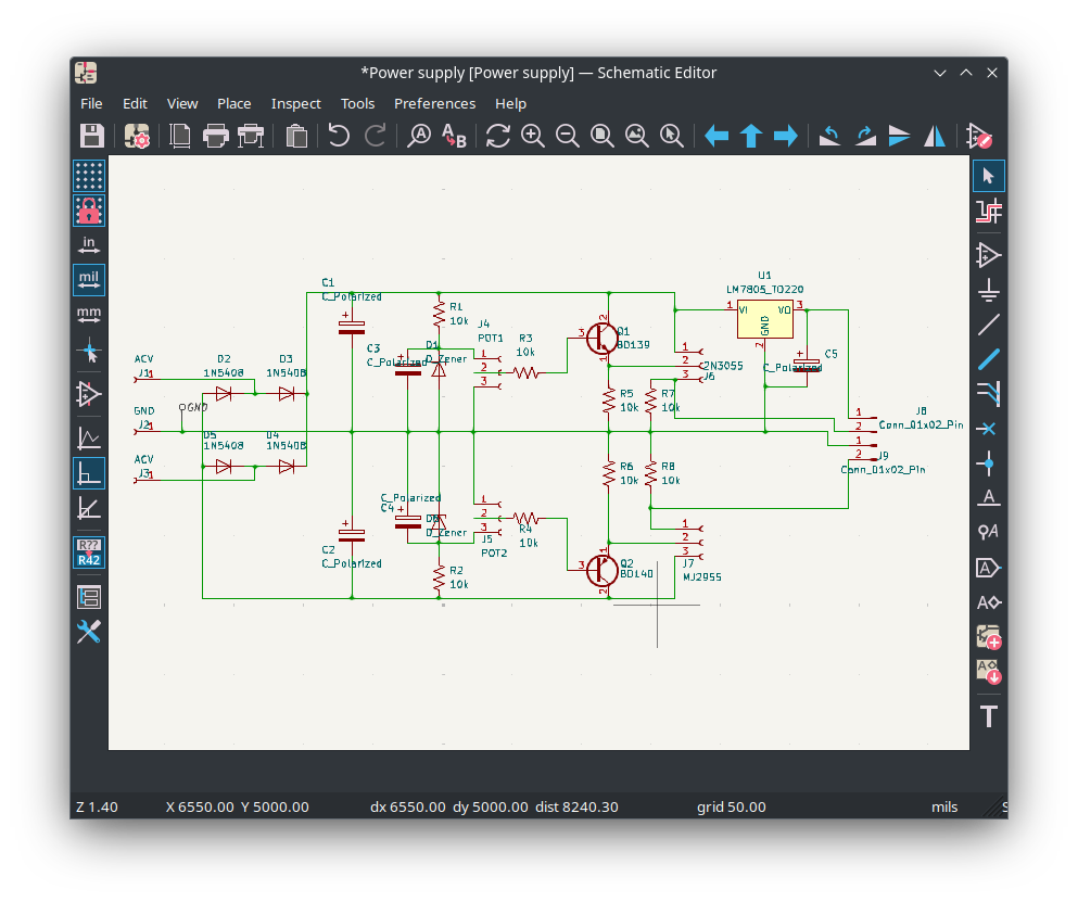
Wire the symbols together — you can do this while adding symbols, or afterwards. Once done, you can move on to the PCB layout; KiCad will prompt you to assign any remaining footprints first.
5. Lay out the PCB
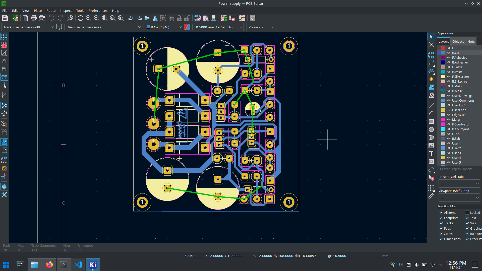
Open the PCB editor (see the pcbnew docs). Arrange your components’ footprints so that the “ratsnest” (unrouted airwire) connections don’t cross each other, using the track, drag, flip, and rotate tools.
A useful order: route everything except ground and VCC first, then route ground and VCC last.
6. Check the result in 3D
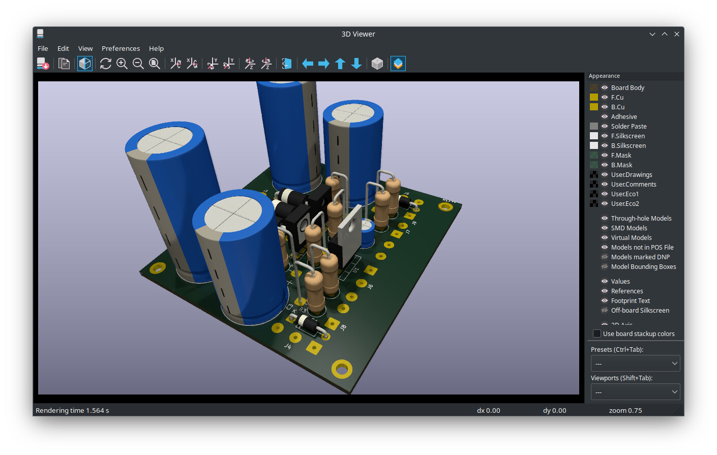
Use the 3D viewer to visually verify your layout before ordering or manufacturing the board.
Related
- How to build an electric safety box for components above 25V — building an electric safety box
Rewritten and consolidated (Sept 2026) from the original student how-to’s: How to Design a PCB (Printed Circuit Board) using KiCad.